|
Observational station and detector
Photoelectric image pipeline Trigger CMOS image sensor |
| Observational station and detector |
The Ashra observational station consists of 12 light collection detectors covering entirely all sky with totally 80 mega pixels in the CMOS sensor arrays. The station site candidates are currently locations near the summits of the three mountains of Mauna Loa, Hualalai, and Mauna Kea on the Hawaii Big Island after taking into account the geometrical distribution for redundant observation ensuring stereo aperture for EHECRs, atmospheric purity, rate of fine weather, low light pollusion, accessibility, and so on (Fig.1).
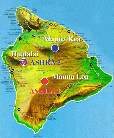
Fig.1 Site (Big Island) In the first step, we are planning to install one full station including 12 detectors at the site near the Mauna Loa summit and 4 detectors in another station on the top of Hualalai which is distant from Mauna Loa by 35km to start up all-sky survey for TeVγ s and precise measurement for arrival directions of EHECRs using stereo fluorescence technique (the Ashra phase 1 project; Ashra-1). In the second step, enhancing the Hualalai site into one full station and installing one another station at the site on the higher side of Mauna Kea to complete the three full stations, we will proceed to discovery and resolve higher energy phenomena in the Universe with lower flux (the Ashra phase 2 project; Ashra-2). We should note that Mauna Loa is the most massive mountain in the world, which is very useful as a detection target for VHEν s. It consists of four smaller sub-detectors viewing the same field to ensure the high sensitivity and the cost-performance(Fig.2). Each of sub-detector utilizes optimized Baker-Nunn optics. We found concrete optical parameters based on the Baker-Nunn optics, which keeps spot size less than 1 arcmin (0.016o) for incident parallel light rays with the incident angles less than 25o. The optical system consists of three corrector normal lenses made of acrylic resin, spherical reflector, focal sphere image intensifire (FIIT) of which size is designed to be roughly φ 1.0m, φ 2.2m, and φ 0.5m, respectively. The light images which are gathered and made independently in the four sub-detector systems are transfered into the following photoelectric image pipeline device together through a light guide. Now the prototype of this optical system with nearly same dimensions as design ones is under fabrication. 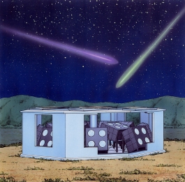
Fig.2 Ashra Sub Detector 
Fig.3 Modified Baker-Nunn optics |
| Return to the top of this page |
| Photoelectric image pipeline |
The photoelectric image pipeline consists of FIIT as described before, light guide, self-triggered IIT (STIIT) providing the functions of splitting light and making optical delay, trigger image sensor, and high resolution CMOS image sensor (Fig.4). Using multiple stage pipeline and light splitter allows us image transportation to the CMOS image sensor with enough gain without sacrificing the fine image resolution and self-trigger for short time phenomena like atmospheric Cerenkov signal. Since the examined resolution at the focal surface is much better than the required one, four light guides after sub-detectors, which can be connected into one STIIT, significantly contributes to high cost-performance of this system. Following the light splitter, a proximity focused IIT is equipped to make delay for the trigger decision time using the scintilation light on phosphor P-46, of which 10%decay-time is 200ns. The gated II after the delay II makes a role of "high speed shutter" by controling the voltage supplied between the photocathode and the micro channel plate (MCP) using the gate signal from the trigger device.
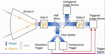
Fig.4 Image Pipeline |
| Return to the top of this page |
| Trigger |
|
The trigger image sensor consists of photocathode, MCP, and 128x128 pad arrays. Each pad receives current amplified by the corresponding area of the MCP and covers about 0.4o field of view. The expected night sky background rate in each pad pixel is about 0.03 photoelectrons every 10ns. Since the Cerenkov light signal from TeVγ induced AS has the transient time of several tens ns including the P-46 phosphor decay time, the high-speed global shutter with the gate II can yield sufficiently high signal-to-noise (S/N) ratio without difficulty.
On the other hand, fluorescence lights from AS induced by VHEν or EHECR has so long transient time of 10 -100 μ s in each trigger pixel field of view that severe night sky background photons are accumulated in each pixel during the AS track in the total field of view and degrade the S/N if the above global control of shutter is used. Another splitter just before the trigger sensor splits the input light into two different trigger image sensors which are independently in charge of discriminating sensed current in each trigger pixel because of the discrepancy of time characteristic of the track image. To keep the trigger rate in each pixel uniform and stable even if there is local effect of night sky background within the field of view, we designed to impliment eight threshold levels including the mask control in each pixel. To select the threshold level, a register is put in each trigger pixel, which is connected via sirial control line for set and reset of the level. The output of the discriminator in each pixel is summed over 64pixels along X and Y directions through wired-or circuits. Actually these additional circcuits are installed under the pixel pad not to reduce the fillfactor of each pad. |
| Return to the top of this page |
| CMOS image sensor |
|
For the CMOS image sensor to achieve 1 arcmin resolution requires more than 2,048 x 2,048 (4M pixels) covering the field of view. It is not so big technical jump. Since the expected trigger rate in each Ashra detector is roughly 1kHz, readout speed must be fast not to make deadtime in the readout system. For this, the function of selective readout is required. Adding that, the observation time for each event in the fluorescence method is so large comparing with the night sky background rate that the 2-dimensional shutters are required which is openned one by one along the AS development on the field of view of the CMOS image sensor. We need to develop this kind of CMOS image sensor, because there is no this kind of image device although a CMOS image sensor with the 1-dimensional shutters so called "rolling shutter" is commercially available. To implement this kind of special function onto the device, the CMOS image sensor is advanced on the points of the easiness and the cost for the development comparing with CCD.
To realize the selective imaging and readout on one CMOS image sensor chip, we have invented the CMOS image sensor with macrocell structure. The number of macrocells is 64 x 64 in one CMOS sensor chip. Each macrocells contains 16 x 16 pixels. As a result, totally 3,072 x 3,072 (9.4M) pixels are implimented on one CMOS image sensor. In the Ashra detector, each sub-detector uses one newly developed CMOS image sensor and each detector uses totally four. |
| Return to the top of this page |